 US
US
 China
China


High-Density Reed Relay Switching: Why Size Is Only Part of the Equation
As test systems and instrumentation demand more channels in less space, the challenge is achieving the highest usable switching density while maintaining accuracy, repeatability, throughput and reliability.
4 × 4 mm
Minimum pitch for Series 120 / 122 / 124
<5%
Operate-voltage change with properly screened close-packed designs
~80 µs
Typical operate and release time for Series 124
0.1 pF
Typical guarded switch-to-coil capacitance with Series 103G / 103GM
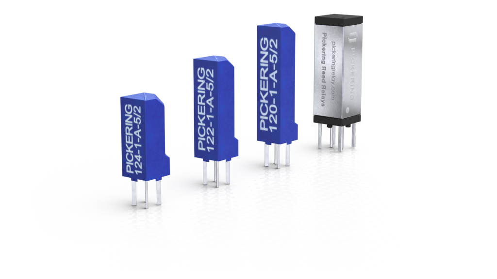
Table of Contents
- What does high-density switching actually mean?
- Consider magnetic interaction when relays are closely packed
- Consider heat and thermal EMF for low-level measurements
- Account for capacitance and signal coupling
- Don’t overlook contact resistance stability
- Switching speed also affects useful density
- Assess density by switching functionality
- High-voltage switching can benefit from compact stacking
- High density demonstrated in real switching systems
- Choose density around the application
When more switching channels need to fit into a limited PCB area, relay size matters.
Pickering has spent decades miniaturising reed relay technology and today offers some of the smallest devices available. The Series 124, for example, is the smallest through-hole reed relay currently available and can be stacked on a 4 mm × 4 mm pitch. For applications requiring more contacts in a compact package, the Series 125 provides two-pole switching within a board area of just 5 mm × 5 mm.
High-density switching introduces a broader set of design considerations once relays are packed closely together.
As automated test equipment (ATE), semiconductor test systems and precision instrumentation accommodate increasing numbers of switching channels, placing relays closer together changes the environment in which those relays operate. Magnetic interaction, coil heating, thermal EMF, capacitance, contact resistance stability and switching speed can all affect the performance of the finished system.
A relay can therefore be extremely small and still be poorly suited to a particular high-density application.
High-density design should maximise usable switching density while preserving the accuracy, repeatability, throughput and reliability required by the application.
What does high-density switching actually mean?
Physical footprint is the most obvious measure of relay density, particularly in applications such as PXI and LXI switching modules where board space is fixed and channel count can be critical.
Pickering’s Series 120, 122 and 124 ultra-high-density relays can all be mounted on a 4 mm × 4 mm pitch. Geometrically, that corresponds to 6.25 relay positions per cm² before PCB routing, driver circuitry, connectors and other components are considered.
- more individual switching channels within a given PCB area
- more poles per relay
- reduced component height
- greater switching power without increasing PCB footprint
- low capacitance for high-speed or wide-bandwidth signals
- low thermal EMF for precision measurements
- high electrical isolation between channels
- fast operate and release times
- predictable operation when large numbers of relays are mounted close together
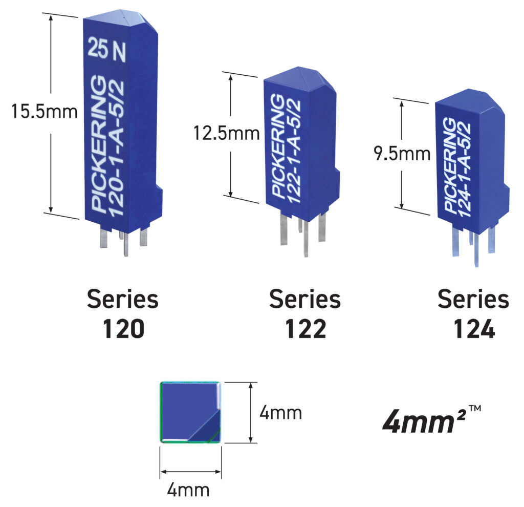
Same 4 mm × 4 mm pitch, different design priorities. Series 120, 122 and 124 offer different package heights and switching capabilities within the same board footprint.
For example, the Series 120, 122 and 124 share the same 4 mm × 4 mm mounting pitch but provide different combinations of package height and switching capability.
The Series 125 takes a different approach. It occupies a 5 mm × 5 mm board area but is available in 1 Form A, 1 Form B, 1 Form C and 2 Form A configurations, providing two normally open switching poles in a single package where required.
Physical size is only one measure of relay density. The more meaningful measure is the electrical performance and switching functionality that can be delivered within the available board area.
1. Consider magnetic interaction when relays are closely packed
Reed relays operate magnetically: current passing through the relay coil creates the field required to operate the reed switch. When several relays are mounted close together, those fields can interact. In an unscreened device, the field generated by one relay can partially oppose or reinforce the field acting on an adjacent relay, changing the coil voltage required to operate the switch and reducing the available drive margin.
Pickering testing has shown increases in operate voltage of up to approximately:
- 40% for unscreened relays
- 30% for partially screened relays
- less than 5% for properly screened Pickering designs
Some devices reduce typical interaction further. Series 125, for example, has a typical magnetic interaction figure of approximately 1% when mounted on its 5 mm pitch.
Increase in operate voltage due to magnetic interaction when relays are closely stacked
Figures based on Pickering magnetic interaction testing. Actual interaction depends on relay type, spacing and operating conditions. For more information on magnetic interaction, read this article .
In practice, magnetic interaction can influence:
- operate and release voltage
- switching time
- repeatability
- coil-drive margin
- operation across temperature and supply tolerances
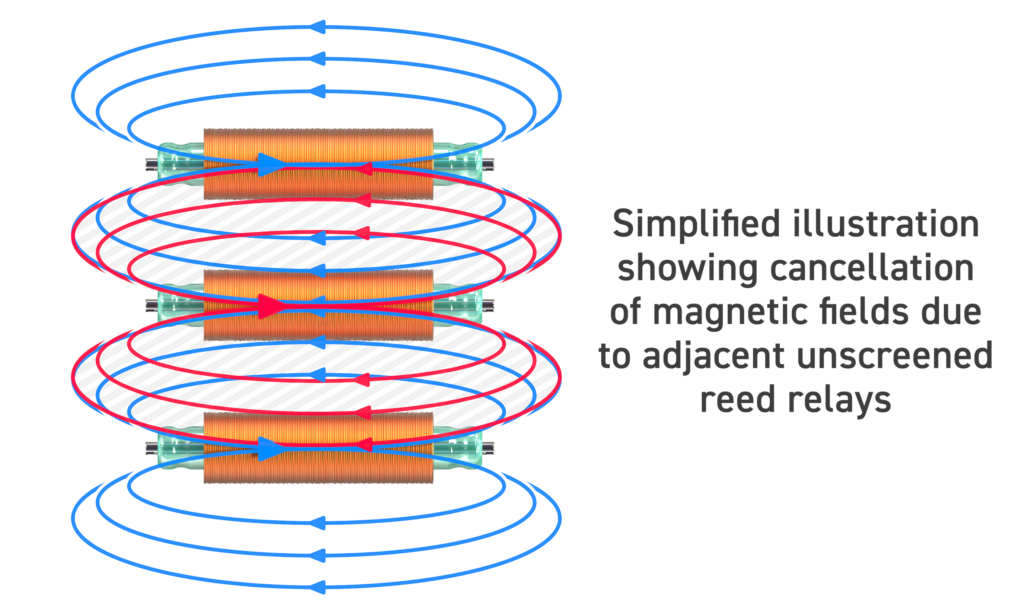
Designing for close-pitch operation
At low channel counts, magnetic interaction may seem like a component-level detail, but in a matrix containing hundreds of relay coils it becomes a system-level design consideration.
2. Consider heat and thermal EMF for low-level measurements
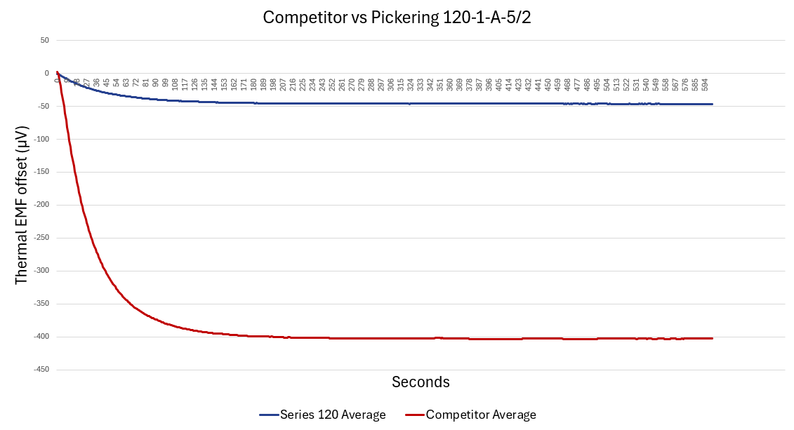
Thermal EMF over time following coil energisation.
The two high-density relays show markedly different thermal behaviour under the same test conditions.
In many switching applications, a few microvolts will have little practical effect. In precision data acquisition, semiconductor test, sensor measurement and low-level DC applications, however, the relay itself can become a meaningful contributor to measurement uncertainty. This makes thermal behaviour particularly important when comparing compact relays, as two devices with similar PCB footprints can produce very different offsets once their coils are energised.
Pickering recently compared its 3.9 mm-wide Series 120 with another 4 mm-class high-density reed relay under controlled conditions. Both coils were energised at nominal voltage and the thermal EMF across the contacts was recorded over ten minutes.
At the end of the test, the Series 120 produced an average offset magnitude of approximately 46 µV, compared with approximately 403 µV for the comparison relay under the same conditions. That’s approximately 8.7:1 difference in final offset magnitude.
Read the full test methodology and results in our article: Not All High-Density Reed Relays Perform the Same
Similar package dimensions do not necessarily mean similar measurement performance.
Where thermal EMF is particularly critical, the optimum design may deliberately trade some packing density for a relay designed specifically for low-level measurement.
Pickering’s Series 100, for example, is designed to provide thermal EMF of approximately 1 µV or less in dry versions, making it suitable for applications including precision data acquisition and thermocouple switching.
The useful density of a switching system therefore needs to be considered alongside the smallest signal it is expected to measure.
3. Account for capacitance and signal coupling
In low-frequency DC applications, these effects may be negligible. For high-speed digital signals, fast pulses and wide-bandwidth ATE matrices, however, parasitic capacitance can affect isolation, rise time, crosstalk and overall signal integrity. Relay construction, magnetic screening, electrostatic guarding and PCB layout therefore need to be considered together as part of the same signal path.
Where low capacitance is a primary requirement, Pickering’s Series 103 is designed to minimise inter-terminal capacitance. The 103/103M versions achieve typical closed switch-to-coil capacitance of around 0.4 pF, compared with around 2.5 pF for a standard SIP/SIL reed relay, while guarded 103G/103GM versions can reduce this to around 0.1 pF when the guard is actively driven.
The guarded Series 103 uses an internal coaxial electrostatic screen and can also achieve approximately 0.08 pF across the open switch contacts. As signal frequency increases, differences of this scale become more significant to isolation, rise time and overall signal integrity.
For high-bandwidth or fast-pulse applications, parasitic capacitance can therefore become a more important selection criterion than absolute package size. The optimum high-density relay is the one that meets the signal-performance requirements of the system within the available space.
This is particularly important in ATE matrices, where multiple signal paths must maintain bandwidth and isolation within a compact switching architecture.
Controlling capacitance at the relay level can also make it easier to meet system-wide bandwidth and isolation targets as channel count increases.
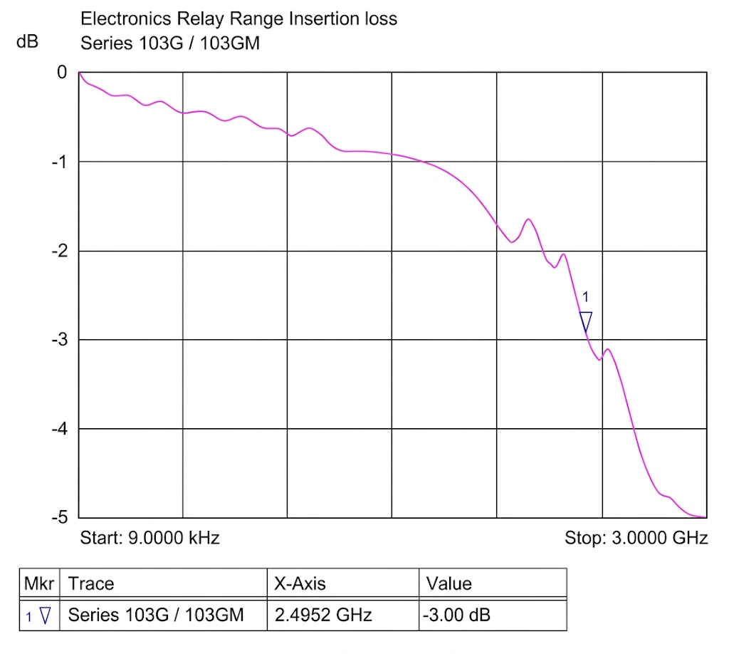
Series 103G / 103GM insertion-loss performance. Measured response illustrates the wide-bandwidth capability of the low-capacitance design.
4. Don't overlook contact resistance stability
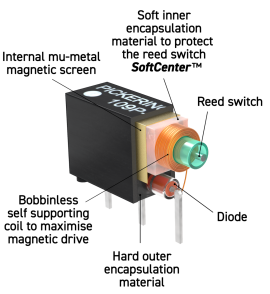
SoftCenter™ construction. Soft inner encapsulation helps reduce mechanical stress on the reed switch and support stable contact performance.
Reed switch blade alignment, contact materials, contamination and mechanical stresses within the package can all influence how consistently the contacts close. Pickering uses instrumentation-grade reed switches and controls the relay construction to support predictable contact behaviour over repeated operations.
Pickering’s SoftCenter™ construction uses a softer encapsulation material around the glass reed switch to reduce mechanical stresses that could otherwise affect blade alignment and contact resistance stability. Pickering relays are also 100% tested for operating parameters, rather than performance being inferred solely from batch sampling.
For precision switching systems, this consistency matters as much as the initial resistance figure. The objective is a switching path whose behaviour remains predictable across repeated operations, changing temperatures and long service periods.
5. Switching speed also affects useful density
Physical channel density only adds value if the switching architecture can meet the throughput requirements of the test system. In automated test, relay operate and release times contribute to the overall test cycle, particularly where large numbers of channels are scanned sequentially.
Pickering’s Series 124 has typical operate and release times of approximately 80 µs, while Series 122 has typical operate and release times of 150 µs or less. The difference is measured in microseconds, but across thousands or millions of switching operations, relay speed can become a meaningful part of the system timing budget. Actual throughput will also depend on measurement settling time, instrument response, software overhead and whether switching operations can occur in parallel.
Switching density should therefore be considered at system level, with relay speed forming part of the overall design decision. An application constrained by enclosure height and test speed may favour the 9.5 mm-high Series 124, while a design requiring greater switching power on the same 4 mm PCB pitch may favour the Series 120.

6. Assess density by switching functionality
Relay count per square centimetre is a useful starting point, but it does not fully describe how much switching capability a design can provide. In applications that require multiple poles, the number of switching functions available within a given board area can be the more meaningful measure.
The Series 125 is a good example. It occupies a 5 mm × 5 mm board area and is available as a 2 Form A relay, allowing two independently operated switching poles within a single package. Geometrically, four Series 125 devices can fit within 1 cm², providing up to eight Form A switching poles per cm² before PCB routing and surrounding circuitry are taken into account.
A 4 mm-pitch single-pole relay, by comparison, provides a theoretical 6.25 relay positions per cm², giving 6.25 Form A switching poles per cm².
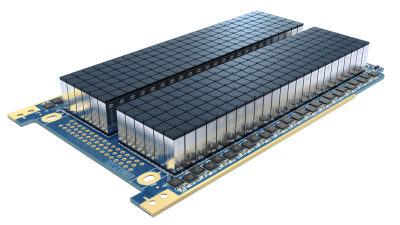
Series 125 in a high-density switching assembly. The two-pole relay provides greater switching functionality within a compact 5 mm × 5 mm footprint.
These figures are a geometric comparison rather than a PCB-layout prediction; practical designs must also accommodate routing, drivers, clearances, vias, connectors and other circuitry. The broader point is that useful density depends on the switching functionality delivered within the available space, particularly in matrices requiring multiple poles, changeover contacts or normally closed contacts.
A more useful measure of switching density is the functionality delivered within the available board area.
That distinction becomes important in matrices requiring changeover contacts, normally closed contacts or multiple poles.
7. High-voltage switching can benefit from compact stacking
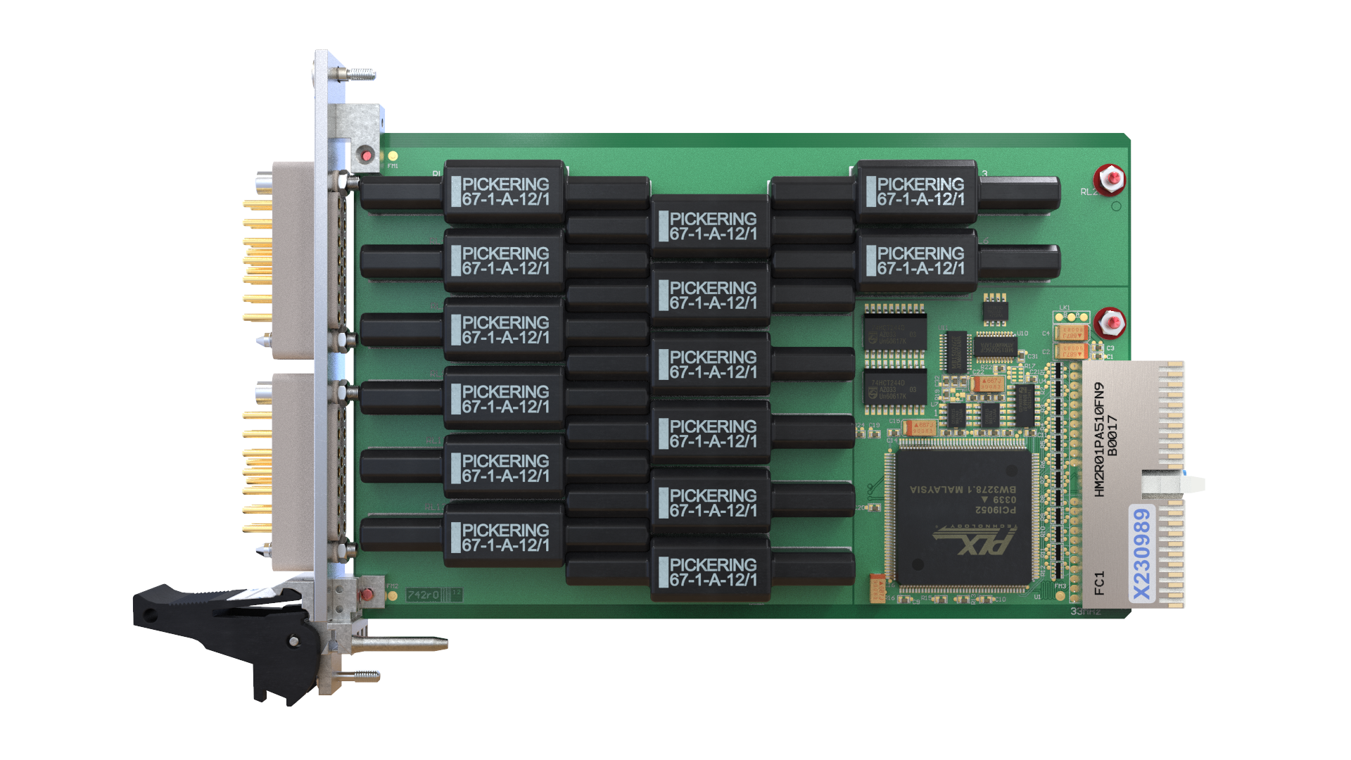
Series 67 high-voltage reed relays stacked on a PCB assembly. The package design supports compact high-voltage switching layouts in matrix and multiplexer applications.
High-density design is also relevant in high-voltage switching, where electrical clearance and the routing of high-voltage connections can place additional constraints on PCB layout. Pickering’s Series 67 and 68 use an unusual Single-in-Line package and former-less coil construction that enables compact stacking arrangements when building high-voltage multiplexers and matrices.
The Series 67, shown here, uses PCB connections for both the switch and coil, allowing the relays to be mounted directly onto the board in compact stacked arrangements. Its unusual Single-in-Line package and former-less coil construction help reduce package size, making it well suited to high-density multiplexers and matrices. Series 67 devices are available with ratings up to 10 kV stand-off and 7.5 kV switching, combining high-voltage capability with efficient use of PCB space.
Working on a high-voltage switching design?
Explore Pickering’s High Voltage Reed Relay Resource Center for relay options, technical guidance and application information for high-voltage switching systems.8. High density demonstrated in real switching systems
The practical measure of a high-density relay is whether it can be deployed reliably at scale.
Pickering reed relays are already used in switching architectures containing hundreds of devices.
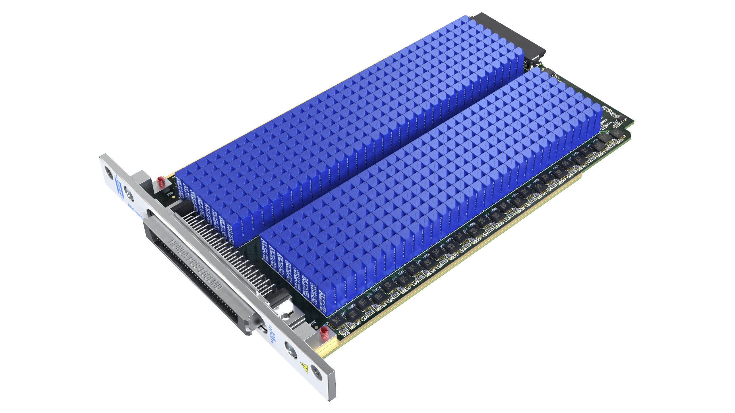
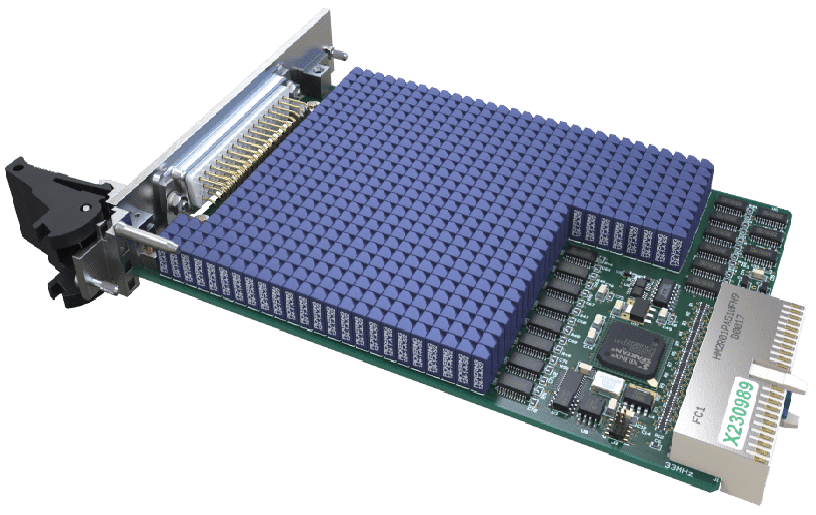
An example Pickering Interfaces ultra-high-density PXI module incorporates 528 Series 122 relays, demonstrating the packing density made possible by the 4 mm-pitch package.
516
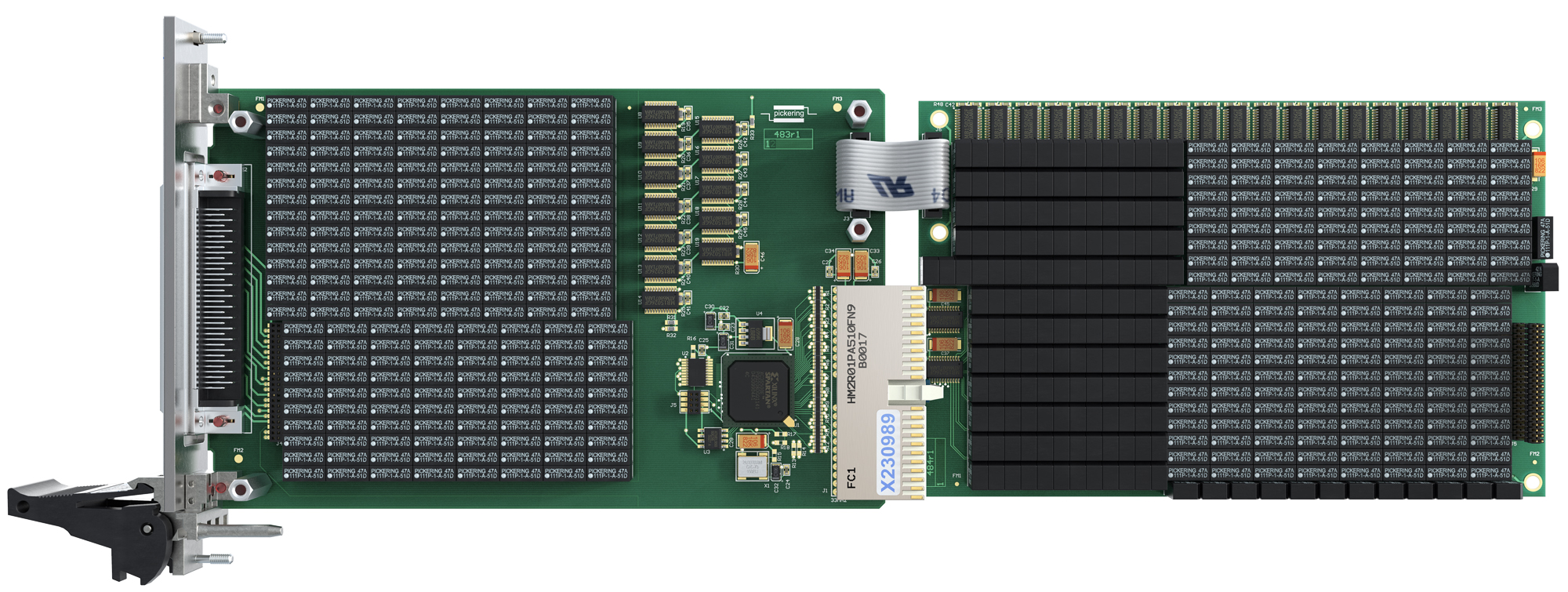
Another Pickering Interfaces high-density matrix module uses 360 Series 111P relays and 156 Series 117 relays. That’s 516 reed relays in total.
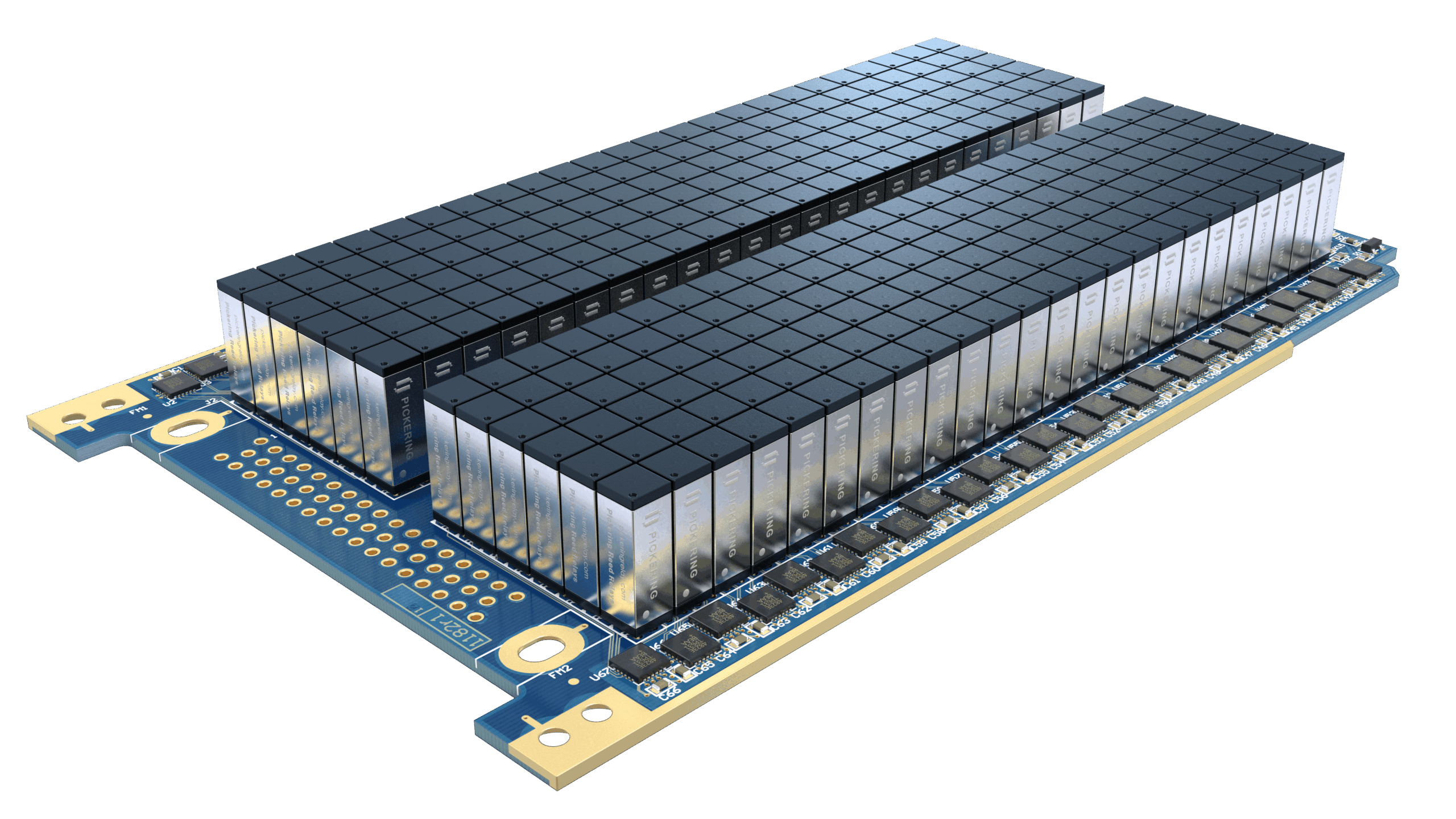
A Pickering Interfaces PXI BRIC matrix daughter card incorporates 288 Series 125 relays.
These examples show that high-density reed relays are already being deployed at scale in real switching hardware. A Pickering Interfaces PXI module using Series 122 relays demonstrates the packing density achievable on a 4 mm pitch, while Series 125 devices provide two-pole switching with typical magnetic interaction of around 1% when closely mounted.
At several hundred relays per assembly, characteristics such as magnetic interaction, thermal behaviour, capacitance, switching speed and contact consistency become part of the overall system architecture. The practical measure of density is therefore how much reliable switching functionality can be delivered within the available space.
8. Choose density around the application
There is no single specification that defines the ideal high-density switching solution. The correct choice depends on what the switching system is expected to do.
Design Priority | Important relay characteristic | Example Pickering solution |
|---|---|---|
Maximum single-pole channel density | Small PCB footprint | Series 120 / 122 / 124 |
Multiple poles in minimum PCB area | Functions per package | |
Very low-level DC measurements | Low thermal EMF | |
Wide bandwidth or fast pulses | Low inter-terminal capacitance | |
Large, closely packed matrices | Effective magnetic screening | Mu-metal-screened ranges |
Higher switching power on 4 mm pitch | Switching current and power | |
Low-profile equipment | Component height | |
High-speed test | Operate and release time | |
Surface-mount assembly | Package technology | |
High-Voltage switching | Switching and stand-off voltage |
This means specifying a switching matrix should begin with the electrical and system requirements rather than relay dimensions.
Before selecting a relay, consider:
- How many switching channels are required?
- Which contact configurations are needed?
- How many relays may be energised simultaneously?
- What voltage, current and power must be switched?
- What is the lowest signal the system will measure?
- Is thermal EMF significant to the measurement uncertainty?
- What bandwidth or rise time must be maintained?
- What level of open-channel isolation is required?
- What PCB area and component height are available?
- What switching and settling times are acceptable?
- Will the contacts normally be hot or cold switched?
- What operating life is required at the actual load?
Once those requirements are understood, physical density becomes one part of the relay-selection process rather than the starting point.
High density without compromising precision
Modern test systems are being asked to deliver more switching channels in less space while maintaining measurement accuracy, repeatability and throughput. Compact reed relays make that possible, but the usable density of a switching architecture depends on more than component footprint alone. Relay construction, electrical characteristics and the way devices behave when closely packed all influence how effectively the available PCB area can be used.
As channel counts increase, magnetic interaction, coil heating, thermal EMF, parasitic capacitance, contact resistance stability and switching speed all become part of the system-level design. Their importance will vary by application: a low-level measurement system may prioritise thermal performance and contact stability, while a high-speed ATE matrix may place greater emphasis on capacitance, isolation and switching time. These effects can become increasingly significant as more relays are brought together within the same assembly.
For designers of ATE, semiconductor test systems, data-acquisition equipment and precision instrumentation, the most useful measure of density is the amount of reliable switching functionality that can be delivered within the available space while still meeting the electrical, measurement and throughput requirements of the system.
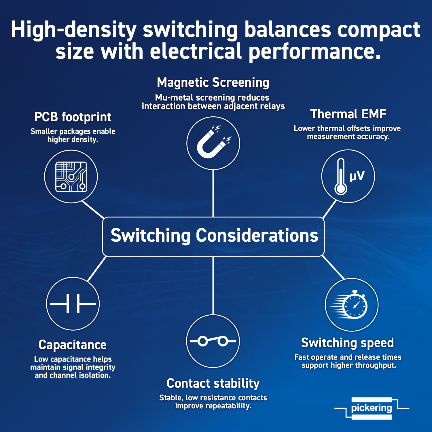
High-density switching balances PCB footprint with the electrical and performance requirements of the application.
Considering these factors together helps ensure that higher channel density translates into practical system performance rather than simply a more compact layout.
That is the difference between fitting more relays onto a PCB and designing an effective high-density switching architecture.
Designing a high-density switching matrix?
Choosing the right relay for a high-density design means balancing channel count, signal levels, switching speed, thermal performance, capacitance and available PCB space. Pickering’s engineering team can help identify the most appropriate relay architecture for your application.
